Mixed-technology assemblies: SMT and through-hole on one board
Most real boards are mixed. A dense surface-mount field sits beside a connector that has to survive cable mating, a transformer that needs a barrel joint, or a shunt carrying 400 A. The engineering question is not whether to mix the technologies but how many process passes it takes — and on recent programs we have taken that from 3 passes to 2 without adding a single tooling item.
- Typical mix
- Under 5 % of placements · over 25 % of touch time
- Board thickness
- 0.4 mm – 6.4 mm
- Process passes
- 3 conventional · 2 with pin-in-paste
- First-pass yield
- 97–99 % on ramp programmes
Why mixed builds go wrong at other suppliers
Mixed technology concentrates risk in the sequence. Four failure modes account for most of the yield lost on this class of assembly, and all four are decided by process order rather than by equipment.
Bottom-side masking that leaks
A wave or selective pass after reflow means the finished SMD side has to be protected. A pallet or tape mask that does not seal lets flux and solder splash onto gold pads, into connector cavities and under 01005 parts. The damage is usually invisible at AOI and shows up as a leakage or intermittency failure at functional test.
Double reflow on the same side
Running the bottom side through a second reflow while the top side is already populated means every top-side joint sees two liquidus excursions. Large area arrays can void more on the second pass, and parts held only by their own solder can drop off if the profile is not derated for the added thermal mass.
Connector damage from heat and handling
Wave contact at 245–260 °C on a plastic connector body that is only rated to 240 °C deforms the housing and shifts the pin position. The joint passes inspection and the mating tolerance is gone. Selective soldering exists precisely to keep that heat local, but it only helps if the pallet is designed around the connector.
Paste-in-hole that never filled the barrel
Pin-in-paste fails in a specific way: the paste prints, the connector seats, the part looks fitted, and the barrel is only partly filled because the paste volume was calculated from the pad area instead of the annulus volume. The result passes visual inspection and fails thermal cycling. It is a calculation error, not a workmanship error.
The process order we use, and the two alternatives
Every mixed assembly runs one of three sequences. The choice sets the tooling, the number of thermal excursions and the inspection plan, so it is fixed at DFM and does not change mid-program.
| Route | Sequence | Passes | Best fit |
|---|---|---|---|
| A · Two reflow plus wave | Top SMD reflow → bottom SMD reflow → wave or pallet | 3 | High through-hole count, open layout, mixed part sizes |
| B · Two reflow with pin-in-paste | Top SMD reflow → bottom SMD reflow with connector paste printed in the same stencil | 2 | Connector pitches of 1.27 mm and above, holes 0.6–1.5 mm |
| C · Reflow plus selective | Top SMD reflow → selective solder robots for the through-hole content | 2 | Thermally sensitive connectors, few joints, dense SMD nearby |
Why route B usually wins on cost
Route B removes an entire pass: no pallet, no wave pot contact, no second handling step for the connector, and one fewer thermal excursion on every joint already on the board. On a 24-up panel with 46 through-hole pins the wave pass is not the expensive part — the pallet, the masking and the re-inspection are.
Route C stays the right answer where the connector cannot see 245 °C, where the joint count is small, or where the through-hole part arrives late and boards must ship. It is also the fallback when a hole is too large for paste to bridge.
What decides route C against route B
Three things: hole-to-pin clearance above 0.5 mm, a connector body rated below the reflow peak, or a hole pattern too dense for a paste overprint. Any of those pushes the build to selective soldering. Where a design uses both — a fine-pitch block that must be selective-soldered and a power connector that can be pin-in-pasted — we run the paste on one and the robot on the other, in the same program.
Pin-in-paste: getting the paste volume right the first time
Intrusive reflow, or pin-in-paste, prints solder paste into the through-hole barrel in the same stencil operation that prints the surface-mount pads. The connector is placed by hand or by machine, and the reflow oven does the rest. It removes the wave step entirely, at the cost of a tighter aperture calculation.
Paste volume is calculated from the annulus, not the pad: the volume of the barrel minus the volume displaced by the pin, multiplied by the target fill fraction, plus the fillet allowance on both sides. Our working target is 60–80 % of the annulus volume on holes with 0.2–0.4 mm diametral clearance, which leaves room for the flux to vent and produces a fillet on both sides without flooding the mask.
Apertures are overprinted onto the solder mask at 1.8–2.5 times the pad area on a 0.15–0.20 mm foil, or a stepped foil up to 0.25 mm in the connector zone where the paste volume cannot be reached otherwise. The paste printed around the pin acts as a gasket: if it does not seal, outgassing during reflow blows through the barrel and leaves a void that X-ray catches and a rework station has to fix.
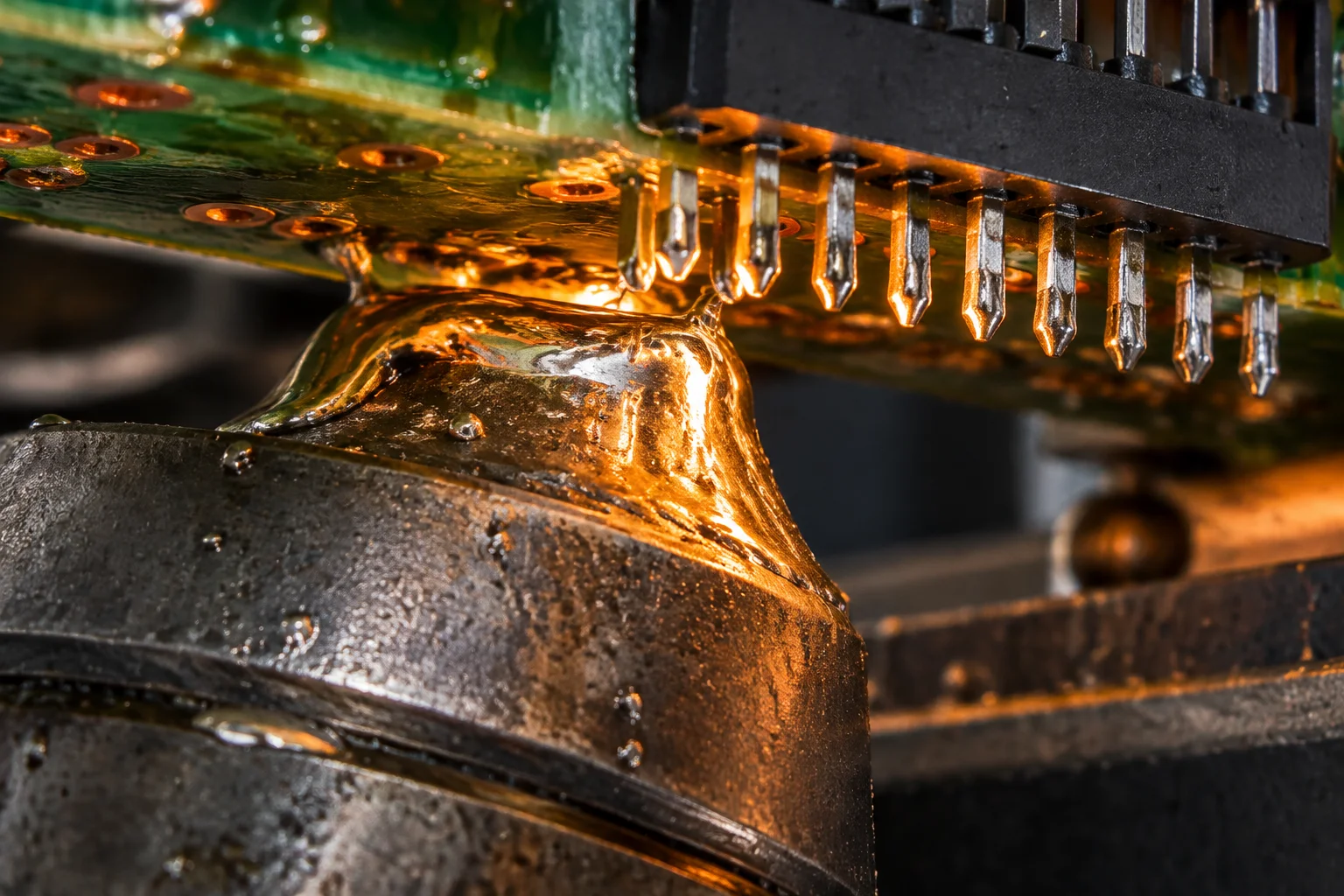
Pin-in-paste needs 0.2–0.4 mm diametral clearance between pin and finished hole. Below 0.2 mm the connector will not seat without pushing paste out of the barrel; above 0.5 mm there is not enough paste in a normal stencil to fill the annulus, and the joint must go to wave or selective soldering. This is a fabrication drawing decision, so it is worth fixing before the bare boards are ordered.
Selective solder pallet design: keep-out, isolation, ramp rate
A selective pallet is a thermal and mechanical tool. Get it wrong and the assembly is soldered correctly while the parts beside it are cooked or cracked.
Keep-out and mask walls
Every joint that must stay dry gets a mask wall 1–1.5 mm thick with 0.5 mm clearance to the pad. Fitted SMD parts sit in milled pockets with at least 1 mm of surrounding material, and the pallet is cut from the CAD data so a revision change is a same-week change.
Isolation between zones
The pallet shields the reflowed side from the nozzle. Top-side temperature in the SMD field is held well below the 217 °C liquidus of the SAC305 joints already made, and the connector body stays under its rated temperature while the barrel reaches 245–260 °C.
3–5 °C/s heating limit
Local heating is limited to a 3–5 °C/s ramp at the joint. Faster than that and the thermal gradient across a multilayer board cracks MLCC terminations and stresses the plated barrels — a failure that passes final test and appears in the field.
First article on every pallet
Each new pallet is checked on the first and last board of a panel: joint fill on the target joints, mask effectiveness on neighbouring SMD (no flux bleed, no solder splash on gold pads), pallet flatness after a full thermal cycle, and a thermocouple trace on the shielded side. Pallets that warp more than a fraction of a millimetre across a run are retired, because a warped pallet is the usual cause of a partly filled barrel on one side of a panel.
Inspecting a mixed board: which joints get which check
A mixed assembly has two joint populations with different physics, so a single inspection method cannot cover both. The plan below is what the control plan specifies per joint family.
| Joint family | Primary check | Secondary check | Acceptance |
|---|---|---|---|
| SMT chip and leaded joints | Inline 3D AOI after reflow | Post-depanel AOI | IPC-A-610 class on the drawing |
| BGA, CSP, LGA, QFN | 2D plus 3D CT X-ray | Cross-section at FAI | Void ≤ 25 % |
| Wave and selective through-hole joints | 2D X-ray barrel fill | Visual fillet, both sides where visible | 75 % minimum vertical fill |
| Pin-in-paste joints | X-ray from the connector side | Micro-section at FAI, then per lot | Both-side fillet, no blow-through |
| Connector retention | Destructive pull test at FAI | Push test on staked parts | Per lead diameter on the drawing |
| Coated or potted units | UV trace inspection of coverage | Ionic contamination ≤ 1.56 µg NaCl-eq/cm² | IPC-CC-830 material spec |
Pull and push testing is destructive, so it is done on first-article and periodic samples rather than in-line. The force criteria come from the connector supplier data or, where none is published, from the lead diameter table in the drawing package.
An eight-layer industrial board that dropped from 3 passes to 2
The board was a 2.0 mm, eight-layer industrial controller with 1,180 surface-mount placements, two 0.4 mm pitch QFNs and a 46-pin power connector on 2.54 mm pitch. It was running the conventional route: top-side reflow, bottom-side reflow, then a palletised wave pass for the connector.
The wave pass was the problem. The pallet masked a 60 × 40 mm area of finished SMD, the connector body saw wave contact at 250 °C even with a heat shield, and every panel needed a manual touch-up on two or three joints after the wave. First-pass yield sat around 97.1 % across the first four lots, with most of the loss concentrated in the masked region.
We moved the connector to pin-in-paste. The stencil was re-cut in the connector zone with a 0.20 mm foil and overprinted apertures at roughly twice the pad area, the paste volume was set from the annulus calculation at 70 % fill, and a support block was added under the footprint so the 46 pins seated evenly. The wave pass, the pallet and the touch-up operation all disappeared.
Cycle time fell by 18 minutes per panel, first-pass yield moved to 99.2 % over the following five lots, and the connector housing stopped showing heat marking. The change cost one stencil and one support block, and it is now the default route we propose for any connector with 1.27 mm pitch or coarser and 0.2–0.4 mm hole clearance. The route comparison is on the through-hole page.

One process pass removed, one pallet retired, 18 minutes of touch time saved per panel, and no reduction in joint acceptance criteria — the pin-in-paste joints still meet the same 75 % vertical fill floor as the wave joints they replaced.
Mixed-technology questions from design teams
Not if the profile is built for it. The second pass sees the added thermal mass of the first side, so the soak is extended and the peak is held at the low end of the 235–245 °C window. Parts that cannot survive two excursions — some electrolytics, most unsealed relays, and a few plastic-bodied connectors — are sequenced to the last pass or moved to selective soldering. We see about one design in ten where a specific part forces the sequence rather than the layout, and it is always cheaper to find that at DFM than after the first build.
Sometimes. It depends on three things you can read off the fabrication drawing: pin-to-hole clearance, hole size and whether the paste can be overprinted onto solder mask without hitting an adjacent pad. If the clearance is within 0.2–0.4 mm, the holes are 0.6–1.5 mm and there is mask area to overprint, we can usually convert with a new stencil, a support block and a paste-volume calculation — no copper change. If the clearance is wider than 0.5 mm, the conversion does not work and the joint stays on wave or selective soldering.
By keeping the wave away from them. Where a wave pass is unavoidable, the pallet masks the connector cavity and a silicone plug or machined cover closes any opening larger than about 1 mm. The rest is process control: flux specific gravity checked every shift, preheat set so the flux is dry before the wave, and an ionic contamination test at or below 1.56 µg NaCl-eq/cm² after cleaning to prove the residue that remains is harmless. If a connector cannot be masked reliably, it goes to a selective robot instead.
Ask us to review the process route
Send the fabrication drawing with the BOM and Gerber set. We will tell you whether your through-hole content should run pin-in-paste, selective soldering or a wave pass — and what each route costs.