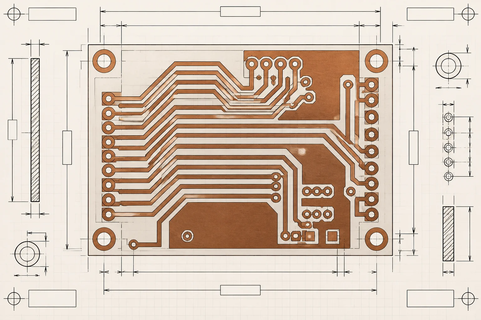
DFM design guides that survive the first build
The working limits we check on every Gerber set — land patterns, panelisation, thermal copper, test access and documentation. Written for the engineer who has to release the layout, not for a brochure.
- Trace / space floor
- 0.10 mm
- Annular ring floor
- 0.15 mm
- Panel utilisation
- 85 %
- DFM turnaround
- 24 hours
A rule set you can check before you release the layout
Every number below is a limit we can build to, plus the value we would choose if the design allows it. Where a rule is a hard floor, the table says so; where it is a preference, it says that too.
These rules are the same list our DFM reviewer works through, in the same order, on every new package. Reading them before you release the layout is worth more than reading them after: a 0.15 mm annular ring that becomes 0.05 mm during a final rip-up costs a fabrication round, and a panel that depanels badly costs a rework station on every unit.
The guide covers the board as it is assembled, not as it is drawn. It assumes FR-4 with 1 oz copper and an ENIG finish unless your drawing says otherwise, a stencil of 0.10 to 0.15 mm laser-cut stainless, and reflow on a 12-zone nitrogen convection oven. If your stack-up or finish is different, say so on the fabrication drawing — the floors move with the process, and we would rather adjust the numbers up front than reject a panel at incoming.
Where a rule conflicts with a compliance requirement, compliance wins and we document the deviation. A creepage distance for a 1,000 V isolated design is not negotiable against panel utilisation, and neither is a Class 3 annular ring.
- Written for
- Layout and hardware engineers
- Applied by
- DFM review within 24 hours
- Density basis
- IPC-7351B nominal
- Stack assumption
- 1.6 mm FR-4, 1 oz copper
- Workmanship basis
- IPC-A-610 Class 2 / 3
Footprints decide yield before the first panel is printed
Most assembly defects that look like process problems are footprint problems. The paste volume a stencil can deposit is set by the aperture you drew, months earlier.
| Density level | Courtyard excess | Fits | Trade-off |
|---|---|---|---|
| Least (L) | 0.10 mm around the land pattern | Dense consumer boards with a rework plan | Least solderable area, highest risk of bridging and tombstoning |
| Nominal (N) | 0.25 mm around the land pattern | Most industrial and medical assemblies at IPC-A-610 Class 2 | The default we recommend when the layout has the room |
| Most (M) | 0.50 mm around the land pattern | Class 3, automotive, and any board that will be reworked | Costs board area and can force an extra layer |
A pad sized for the nominal package
Land patterns copied from a nominal datasheet drawing leave no room for placement tolerance. Extend the pad beyond the package body by the toe fillet the class requires, and check it against the manufacturer's recommended pattern rather than the pin pitch.
A courtyard that overlaps the neighbour
Two parts with overlapping courtyards cannot both be placed to the centre of their tolerance band. The result is a placement offset that shows up as tombstoning on 0402 and 0201 chips and as a lifted lead on a fine-pitch device.
A thermal pad printed solid
A QFN or DFN thermal pad printed with a single full-area aperture floats on its own paste and voids heavily. Split the deposit into a windowpane or dot pattern covering 50 to 80 % of the pad, and keep the area ratio above 0.66 so the paste releases from the stencil.
The seven features that stop a build
Typical is what a competent design uses. Floor is the limit we can build without a deviation, and it assumes the fabrication house holds the tolerance it quoted.
| Feature | Typical design | Our floor | Why it matters |
|---|---|---|---|
| Trace width and space | 0.15 mm / 0.15 mm | 0.10 mm / 0.10 mm | Below 0.10 mm the etch tolerance eats the yield, and the copper thickness needed for current derates the spacing further |
| Annular ring | 0.25 mm | 0.15 mm | Drill wander and plating consume the ring; a breakout breaks the connection and fails IPC-A-610 Class 3 outright |
| Via drill and pad | 0.30 mm / 0.60 mm | 0.20 mm / 0.45 mm | Drill aspect ratio and plating throw drive the minimum; a 0.20 mm drill in a 1.6 mm board is an 8:1 aspect ratio |
| Hole to copper | 0.25 mm | 0.20 mm | Resin recession and drill registration move the copper wall; too little clearance produces a short after thermal cycling |
| Solder-mask dam | 0.15 mm | 0.10 mm | A dam narrower than 0.10 mm lifts or washes away, and the exposed copper becomes a bridging site during reflow |
| Silkscreen over pad | 0.10 mm clear | 0.00 mm — never | Ink on a land keeps solder off the pad; the print file must clip the legend, not rely on the printer |
| Component to board edge | 1.00 mm | 0.50 mm | Router and V-score stress travels into the nearest joint; a chip placed inside 0.50 mm of the edge cracks at depanel |
Annular ring is measured after plating, on the finished hole, at the worst-case registration — not on the CAD data. If your layout tool reports a 0.13 mm ring from a nominal drill table, assume it will build at 0.10 mm and give it another 0.05 mm.
Panel design decides how the board leaves the panel
Panelisation is a cost and quality decision at the same time: it sets the material you buy and the damage you risk at depanel. Our board envelope runs from 20 × 20 mm to 610 × 510 mm.
Rails are 5 mm minimum and 8 mm is the better choice: conveyor rails need enough material to grip, and tooling holes need somewhere to live. A panel without tooling holes or fiducials cannot be placed accurately, no matter how good the mounter is.
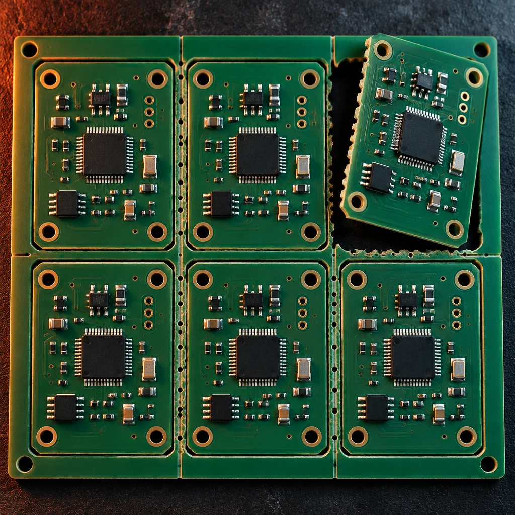
Three breakaway methods cover almost everything. Mouse-bite perforations suit irregular outlines and mixed board shapes, with 0.50 mm holes on a 1.00 mm pitch leaving a controlled web. V-score suits straight-line rectangular boards and long runs, but it consumes panel area and leaves a visible edge that no component may cross. Tab routing with a 3 mm to 5 mm tab and a router bit gives the cleanest edge — we remove the resulting 0.50 mm burrs as a standard step.
Bad panels fail the same three ways: boards rotated 90° from each other so the stencil cannot be shared, components placed within 3 mm of a V-score line, and panels sized so the last board in the row hangs off the conveyor support. All three are visible in the panel drawing, which is why we ask for it before we quote tooling.
| Method | Best for | Limits | Edge condition |
|---|---|---|---|
| Mouse-bite | Irregular outlines, mixed board shapes in one panel | Perforation web of 0.50 mm; components stay 1.00 mm clear of the hole row | Small nibs remain and are hand-finished |
| V-score | Rectangular boards in high volume on straight lines | Score line must run edge to edge; 3 mm component keep-out from the line | Clean straight edge, visible score witness |
| Tab routing | Complex outlines, heavy boards, tight edge tolerances | Tab width 3 mm to 5 mm; router entry needs clearance on the panel | Burrs removed to 0.50 mm as a standard step |
Copper area is a thermal decision before it is a current decision
A trace that carries the current but runs 60 °C hot will fail whichever qualification test comes next. Width is only half of the answer; the other half is where the heat goes.
On 1 oz outer copper, allow roughly 1 A per 1 mm of trace width for a 10 °C rise, and halve that on an inner layer where the laminate cannot dissipate as freely. A 400 A bus is not a trace at all — it is a busbar, a heavy-copper plane or a bolted connection, and the layout should say which one before the copper weight is chosen.
Thermal vias move heat from a pad into an internal plane. A practical array uses 0.30 mm drills on a 0.80 mm pitch, plated through, with the vias either filled and capped or tented from the underside so the paste does not wick down the barrel during reflow. Arrays under a power pad want 50 to 80 % paste coverage for the same reason as any other thermal pad.
Keep-out matters around large parts because a 20 mm inductor or a 55 mm connector absorbs heat from the surrounding board. Give those parts extra copper to preheat against, keep small chip components at least 3 mm away where the layout allows, and expect the profile to be re-tuned: heavy copper and large thermal masses need a longer soak and a slower ramp than a 1 oz signal board.
A board with 3 oz copper on both sides and a 4 mm aluminium-backed section will not follow a standard profile. Our 12-zone nitrogen oven holds ±1.5 °C of profile repeatability, which is what makes a heavy-board profile reproducible batch to batch — but the profile still has to be developed with thermocouples on the real assembly, not inherited from a similar board.
| Item | Value we design to |
|---|---|
| Outer copper, 1 oz | 1 A per 1 mm at 10 °C rise |
| Inner layer, 1 oz | Halve the outer value |
| Thermal via drill | 0.30 mm on a 0.80 mm pitch |
| Paste coverage on a thermal pad | 50 % to 80 % |
| Component keep-out from a large part | 3 mm where the layout allows |
Test access is cheaper to add now than to fixture later
A fixture can only touch what the layout exposes. Test points cost board area; a missing test point costs a functional fixture, a longer test cycle and a bigger escape risk.
Plan for 1.00 mm minimum test pads on a 2.54 mm pitch, on one side of the board only, with a 1.00 mm keep-out ring free of solder mask, silkscreen and tall parts. Probe access from one side means a single fixture and a single pass; probing both sides doubles the handling and the fixture budget.
Where a design has no room for test pads, boundary scan is the alternative — but it only covers the interconnect between JTAG-capable devices. Power rails, analog front ends, connectors and anything downstream of a non-JTAG device still need a probe, a header or a functional test harness. Decide which nets you are happy never to test, and write that decision into the test specification rather than discovering it during fixture debug.
Also keep the fixture in mind when you place tall components: a 25 mm electrolytic capacitor next to a probe field forces a cut-out in the support plate, and a cut-out under a fine-pitch device is how boards crack during test.
| Item | Rule |
|---|---|
| Test pad diameter | 1.00 mm minimum |
| Pad pitch | 2.54 mm preferred |
| Keep-out around a pad | 1.00 mm, mask and legend free |
| Probe side | One side only |
| Board support under a probe field | Continuous, no cut-outs |
The package we need to quote without guessing
A quote returned in 48 hours assumes the files are complete. Missing items push the review into a query loop, and the schedule moves by days, not hours.
- Gerber data in RS-274X, one file per layer, with the layer names stated
- Excellon drill file, plated and non-plated separated and stacked
- IPC-356 netlist for electrical test and for fixture generation
- BOM with manufacturer part number, package, tolerance and temperature grade
- Assembly drawing with polarity, reference designator to silkscreen mapping
- Fabrication drawing: stack-up, copper weight, finish, impedance targets
- Panel drawing, or a written instruction to panelise on our standard rail
- Workmanship class, conformal coat requirement and marking or serialisation rules
- Test specification, with any nets you accept as untested named explicitly
A DFM report inside 24 hours listing every deviation from the rules on this page, ranked by what it costs to fix, with the recommended change and the class reference behind it. Nothing is changed in your files: we mark up, you decide, and the layout stays yours.
If a file is missing we say so on the same day and quote the rest. That is faster than a complete quote that arrives after a two-day email thread about which revision of the drill file is current.
Layout questions we answer most often
Yes, at 0.10 mm / 0.10 mm with 1 oz finished copper and a fabrication house that holds the etch tolerance. Two things make it fail more often than the etch: copper weight, because 2 oz derates the achievable spacing by roughly the thickness it adds to each sidewall, and via count, because every via consumes annular ring that has to come out of the same space. If the design has to be 0.10 mm all over, keep the copper at 1 oz and the finish flat.
Castellations are half-plated holes on the board edge, so they are routed after plating, and the plating has to survive that cut. Specify the finished hole diameter, keep at least 0.20 mm of wall after routing, leave the castellation free of solder mask on both sides, and put the breakaway tab so the router does not tear into a castellation. Include the castellation pattern in the fabrication drawing — it cannot be inferred from the drill file alone.
Rigid-flex runs on the same SMT lines, with three extra rules. Keep vias and plated through-holes out of the bend zone. Set the bend radius to at least 10 times the total flex thickness, and state it on the drawing. Coverlay openings have to be sized so the stiffener and the coverlay do not lift during reflow. Flex assemblies also need their own handling fixtures, because a flexible panel will not sit flat on a conveyor without support.
Send the layout. Get a marked-up DFM report in 24 hours.
We check gerbers, drill, netlist and BOM against the rules on this page and return the deviations ranked by cost, with the class reference behind each one. Your files are not modified.