Test and inspection: AOI, X-ray, in-circuit and functional
Every board passes three inline 3D AOI gates and a 3D SPI gate before it is allowed to reach a functional fixture. X-ray verifies what optics cannot see, and the test result is stored against the board serial number for 10 years.
- Inline AOI gates
- 3 per line
- X-ray
- 2D + 3D CT
- BGA void limit
- ≤ 25 % per IPC-A-610
- Record retention
- 10 years
Each gate exists because the one before it cannot see something
Inspection is placed where the defect is created, not where it is convenient. A paste defect caught at SPI costs one print cycle; the same defect caught after reflow costs a rework station and a reflow pass.
-
Gate 01 · before placement
3D SPI on the printed deposit
Volume, area, height and offset are measured on 100 % of boards against the stencil aperture. The CpK ≥ 1.67 gate is a stop condition, not a report: a line that misses it is corrected before the first component is placed. SPI cannot see a component, which is the whole point of running it first.
-
Gate 02 · after placement
Pre-reflow AOI
Presence, absence, polarity, rotation and offset are checked while the paste is still wet. A missing 0201 or a reversed diode is removed with tweezers here rather than desoldered later. This gate cannot judge a solder joint because none exists yet.
-
Gate 03 · after reflow
Post-reflow 3D AOI
Fillet shape, wetting angle, bridging, tombstoning, billboarding and lifted leads are evaluated against IPC-A-610 criteria for the class on the drawing. Optical inspection cannot see under a BGA, a QFN thermal pad or a shielded inductor — those parts are routed to X-ray automatically by the inspection program.
-
Gate 04 · after X-ray review
2D and 3D CT X-ray
Ball grid arrays, chip-scale packages, land grid arrays and QFN thermal pads are imaged for voiding, bridging, missing spheres, head-in-pillow and package cracking. Voiding is accepted up to 25 % per IPC-A-610, with tighter limits where your drawing calls for them.
-
Gate 05 · after depanel
Post-depanel AOI
Router burrs, chipped edges, cracked ceramic capacitors, lifted pads and flexed breakaway tabs appear only after the panel is separated. Running the same optical gate again after depanel catches mechanical damage that no pre-depanel inspection can predict.
-
Gate 06 · after cleaning
Ionic contamination test
Cleanliness is measured, not assumed. Aqueous-cleaned assemblies are tested to 1.56 µg NaCl-eq/cm² or better per J-STD-001, with the result recorded per lot. AOI cannot detect a conductive residue; only an extraction test can.
Reading a solder joint from the inside out
Two-dimensional X-ray answers whether solder is there. Three-dimensional computed tomography answers whether it is connected, and how much of the joint is void.
| Signature | What it means | Action |
|---|---|---|
| Void above 25 % of ball area | Outgassing trapped during reflow, usually a profile or paste-volume problem | Quarantine the lot, re-check the profile with thermocouples, cross-section a sample |
| Head-in-pillow | Ball and paste did not coalesce; the joint looks present in 2D and is open in CT | 3D CT slice through the ball height, then a destructive cross-section to confirm |
| Missing or displaced sphere | Placement drop, paste slump or a package handling defect | Route the assembly to rework under IPC-7711/7721 with a documented procedure |
| Package crack or delamination | Thermal or mechanical damage, often after baking or depanel | Reject, notify the customer, and trace the assembly back to its reel and date code |
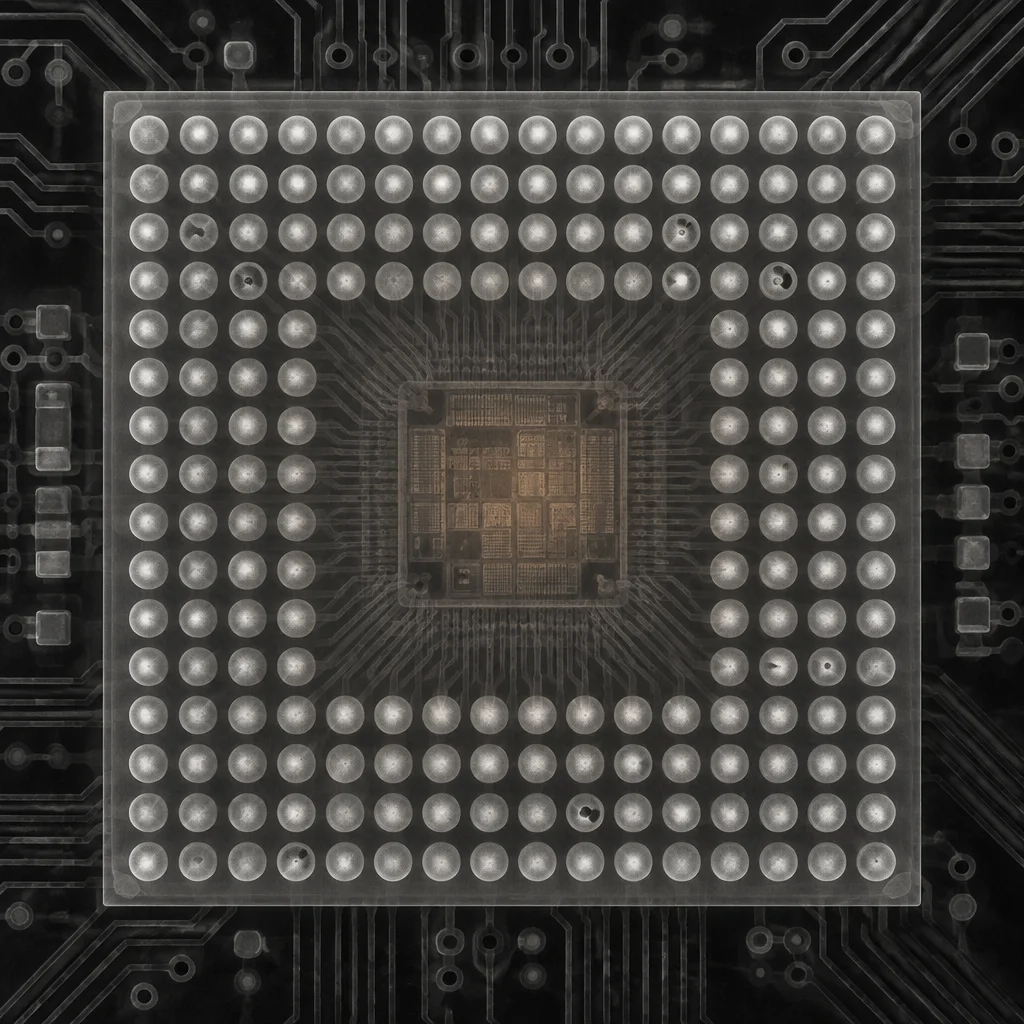
A cross-section is called for on every new product introduction, on any lot that fails an X-ray limit, and whenever a joint's internal grain structure matters to the customer's qualification. Sections are potted, ground and polished to a documented plane and delivered with a measured intermetallic thickness and a photo set at a stated magnification.
Proving a board works: which electrical test pays at which volume
No single method covers everything. The choice is driven by volume, by how many nets are accessible, and by what a field failure costs your customer.
| Method | Coverage | Fixture | Time per board | Worth it when |
|---|---|---|---|---|
| Flying probe | Shorts, opens, component presence and value on accessible nets | None — program only | Minutes, and it scales with net count | 5 to 50 boards, or a design that changes every build |
| In-circuit test | Powered and unpowered measurement of most nets, plus device programming | Bed-of-nails, built in-house | Seconds per board | 500 boards and above on a stable design |
| Boundary scan | Interconnect between JTAG-capable devices; no physical test points needed on those nets | Edge connector or a short header | Seconds, and it can run in parallel | Dense boards with fine-pitch devices and no room for probes |
| Functional test | The product's own specification — inputs, outputs, timing, communication, load | Custom fixture with harness and load bank | Seconds to minutes depending on the sequence | Every shipped assembly, because it is the only test the customer's customer will repeat |
On most programmes we run two of the four: boundary scan or in-circuit test for structural coverage, then functional test for the specification. Running only functional test hides structural defects that pass at room temperature and fail three months later.
Fixtures designed and built in the same building
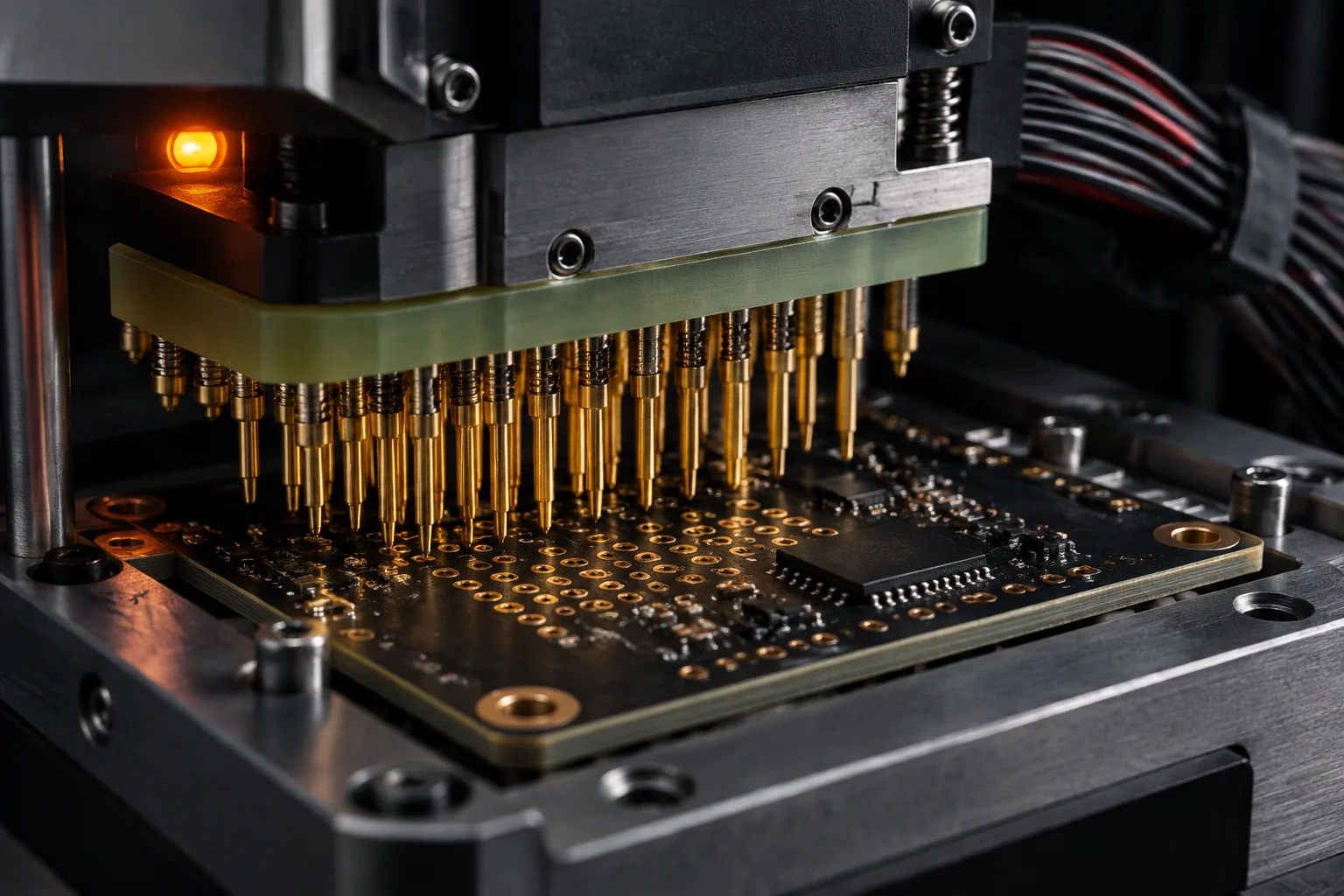
A test fixture is a mechanical design problem with an electrical answer. Building it in-house means the fixture, the program and the first article move on one schedule.
Probe budget, travel, board support and keep-out are checked at DFM stage, before the layout is frozen. A probe needs a flat, solder-mask-free target, enough surrounding clearance for the barrel, and a support point underneath so the board does not flex under load. Test points smaller than 1.0 mm, or placed under a tall component, drive up the fixture cost and the false-fail rate.
Standard spring probes run at a few ounces of force each; a 600-probe fixture therefore applies a substantial load that has to be reacted by a rigid support plate. High-current rails use blade probes or bolted terminals rather than a signal probe, and radio-frequency paths use coaxial probes with a defined ground return so the measurement is not the fixture's characteristic impedance.
Fixture design and build follow the NPI cadence — a pilot run 15 working days after DFM sign-off. Fixture NRE is quoted separately and credited against the programme at 5,000 units, and the customer owns the fixture, the program and the documentation after first article.
Every test result belongs to one serial number
A pass or fail is only useful if it can be tied to the material and the process that produced it.
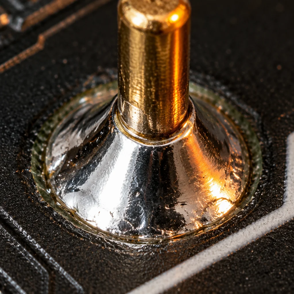
Boards are serialised at the point of first process step, and the MES record carries the stencil, the paste lot, the reflow program, the AOI and X-ray results, the fixture test data and the operator for each step. Test data is retained for 10 years in the IPC-1782 style record set, so a field return can be traced back through the build and out to the component reels it was kitted from.
For functional test we write the sequence, the limits and the fixture wiring document, then hand the source to you with the fixture after first article. Pass and fail limits are version-controlled: a limit change is a documented change with a first-article verification, never an edit made at the station to make a marginal board pass.
Assemblies that arrive already built can be tested here as well. We ask for the test specification, a known-good sample and a known-bad sample where one exists, then run the same records and the same acceptance rules as a board we built ourselves. Read how test-point rules decide fixture cost
Environmental screening before a board goes into the field
Some failures only appear after temperature. Screening moves that discovery into the plant, where it costs a rework instead of a service call.
Temperature cycling and burn-in
Chambers run from 40 °C to 125 °C with programmed ramp and dwell, and units are powered and monitored during the soak where the specification requires it. Burn-in profiles are written per programme and recorded per serial number.
HALT and HASS through partners
Highly accelerated life testing, and the production screen derived from it, run through a qualified partner network. We supply the assemblies, the fixture interface and the failure analysis; the partner supplies the chamber and the vibration table.
Residue and coating integrity
Ionic contamination is tested after cleaning to 1.56 µg NaCl-eq/cm² or better per J-STD-001, and conformal-coated assemblies are inspected for coverage, voids and adhesion under IPC-CC-830 before release.
Test questions that decide a purchase order
Structural coverage comes from AOI on 100 % of boards, X-ray on every ball-grid, chip-scale and land-grid device, and in-circuit or boundary-scan test where the design allows. Functional test then runs your specification. We state which nets and which functions are covered in the test specification document, including the ones that are not testable with the current layout — usually power planes, internal device nodes and nets with no accessible test point.
Yes. After first article the customer owns the fixture, the program and the documentation, and we will ship all three on request. They stay calibrated and maintained here while the programme runs, and we hand over the wiring list, the limit file and a known-good assembly so another site can reproduce the same result without re-developing the test.
We do, with conditions that protect both sides: a written test specification, a known-good sample, and a statement of what happened before the assemblies arrived — storage, prior rework, exposure to moisture. Assemblies that arrive in unsealed packaging with an unknown exposure history are baked at 125 °C for 24 hours before any reflow rework, and the lot is marked as customer-supplied on the record.
Send the assembly drawing and the test specification together.
We will come back with a fixture concept, a coverage statement, the limits we propose and a price — inside the 48-hour quote window, before any fixture is built.