The failure mode: a junction that runs 40 °C above the simulation
The thermal spreadsheet said 78 °C junction at full load in a 40 °C ambient. The thermocouple on the first article said 118 °C. Nothing was broken, nothing was undersized by the datasheet, and the design had passed every electrical check — it simply had a heat path that existed on paper and not in copper.
Almost always the missing path is the one under the device. A power stage dissipates through its thermal pad, through the solder joint, into the copper under the pad, through the board, and out of the far-side copper into air or into a heatsink. If that path is a single signal-layer pour with a handful of untented vias and no far-side copper, the junction sits on a thermal island. The datasheet θJA figure assumes a specific test board — usually a JEDEC 2S2P board with a large copper area — and a real assembly rarely matches it.
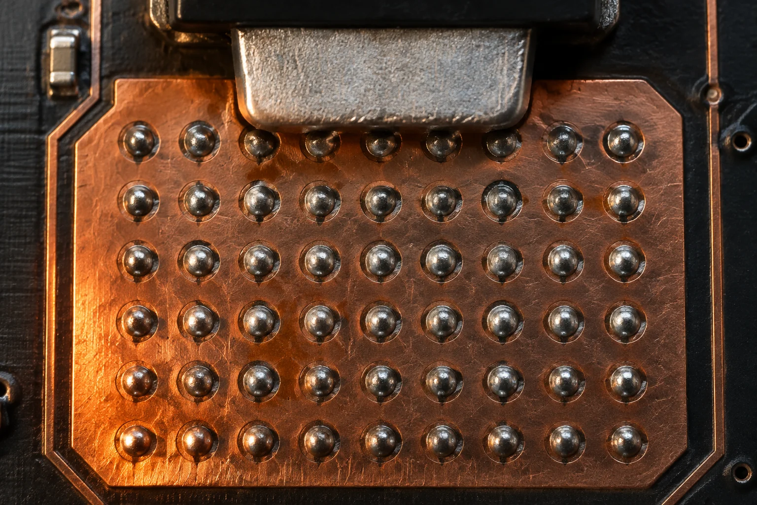
The engineering question is therefore not “how many vias” but “what thermal resistance does the path need to hit the junction temperature target, and what is the cheapest copper geometry that delivers it”. That is a calculation, and it can be done before layout.
Copper area per amp on 1 oz and 2 oz foil
Start with the current path, because it sets the copper weight. IPC-2152 is the current-carrying standard to design against; it supersedes the older IPC-2221 charts because it accounts for board thickness, copper area and the presence of planes, all of which move the answer substantially. As a first-pass rule from the IPC-2221 charts, an external 1 oz trace with a 10 °C rise carries roughly 1 A per 0.5 mm of width, and the same current on an internal layer needs about 2.5 times that width because the laminate conducts heat far worse than air does.
Copper weight buys current capacity but not linearly. Moving from 1 oz (35 µm) to 2 oz (70 µm) roughly halves the sheet resistance and, at the same temperature rise, carries about 1.4 times the current in the same width — the extra copper also spreads heat sideways, which is why the improvement is better than simple resistance scaling suggests.
| Current | 1 oz (35 µm) | 2 oz (70 µm) | Internal layer, 1 oz |
|---|---|---|---|
| 1 A | 0.5 mm | 0.4 mm | 1.2 mm |
| 3 A | 1.4 mm | 1.0 mm | 3.5 mm |
| 10 A | 6.5 mm | 4.5 mm | — |
| 20 A | 16.0 mm | 11.0 mm | — |
Read the bottom two rows before choosing copper weight. A 20 A rail on 1 oz needs a 16 mm wide trace at a 10 °C rise, which on a dense board is often impossible; that is the point where a 2 oz layer, a busbar, or a copper-filled heavy-copper layer becomes the cheaper answer. Above roughly 30 A, no reasonable trace geometry survives — that is busbar territory, and it is why energy-storage and motor-drive designs so often end up with a laminated bus and a bolted connection rather than a wide trace.
Allow for the fact that current does not stay in one layer. A via carrying 20 A must have enough barrel cross-section for the current as well as for the heat: a 0.3 mm drill with 25 µm plating has a copper cross-section of about 0.024 mm², which is roughly a 0.1 mm wide 2 oz trace. That is fine for a signal via and hopeless as a power feed. Power vias get 0.5 mm to 0.8 mm drills, or several of them in parallel.
Thermal via arrays: drill, plating, fill and the void limit
A via is a thermal resistor. To a first order, its resistance from one side of the board to the other is R = L / (k · A), where L is the board thickness, k is the thermal conductivity of the barrel — 0.385 W/(mm·K) for electroplated copper — and A is the copper cross-section of the barrel, which for a plated hole is the circumference times the plating thickness.
Put numbers in. On a 1.6 mm board with 25 µm of plating:
- A 0.3 mm drill has a barrel cross-section of π × 0.3 × 0.025 = 0.024 mm², giving 176 K/W per via. Twenty of them in parallel give 8.8 K/W.
- A 0.5 mm drill has a cross-section of 0.039 mm², giving 106 K/W per via. Twenty-five of them give 4.2 K/W — half the resistance for the same grid area, because the circumference is larger and the drill spacing barely changes.
- On a 2.0 mm board the same 0.3 mm via rises to 220 K/W, so a thicker board needs more vias for the same result. A 6.4 mm board is not a candidate for via-based cooling at all; it needs a copper coin or a metal-core construction.
Add spreading resistance on top. The barrel model ignores the fact that heat has to travel sideways through the pad into the via field and out of the far-side copper, which typically adds 1 to 3 K/W to a real array. Treat the calculated number as the floor, then verify with a measurement.
Fill type changes the resistance materially and is worth arguing about with your fabricator. IPC-4761 defines the via protection types, from Type I (tented) through Type VII (filled and capped). A tented via keeps most of its barrel, but it can wick flux and leave an air void that adds interface resistance. A via filled with a thermally conductive epoxy drops the barrel resistance contribution and adds a conduction path through the fill itself; filled with copper paste it is better again, at a real cost premium. The rule we work to: fill and cap any via in a thermal pad or under a BGA where paste could wick through, and never leave an open via in a pad that has to hold a 25 % void limit under IPC-A-610 — an open via is a direct path for solder to run down the barrel and out of the joint.
Via in pad on a 1.0 mm pitch grid with 0.3 mm drills, offset so that no via sits on the paste aperture line, spreads heat more evenly than a tight cluster in the middle and gives the paste somewhere to go. Increasing the count from 9 to 25 vias in the same pad takes the array from 19.6 K/W to 7.0 K/W without changing the board.
Paste volume on large pads and the void problem
A thermal pad is the hardest paste deposit on the board. It has a low area ratio because it is large, it has vias underneath that pull paste away from the joint, and it outgasses flux volatiles from the centre outward during reflow. The result is voiding, and voiding is measured against the 25 % limit in IPC-A-610 with a tighter negotiated limit on some programmes.
Paste coverage on a thermal pad is deliberately not 100 %. We specify 50 % to 80 % coverage in a windowpane pattern of apertures rather than one large opening, for three reasons: each aperture keeps its own area ratio high enough to release properly, the gaps give flux volatiles an escape route so they do not form blisters, and the paste that does print is spread evenly instead of pooling in the centre.
| Pad size | Aperture pattern | Paste coverage | Expected voiding |
|---|---|---|---|
| 3 × 3 mm | 4 windows of 1.3 × 1.3 mm | 75 % | ≤ 10 % |
| 5 × 5 mm | 9 windows of 1.5 × 1.5 mm | 81 % | ≤ 15 % |
| 8 × 8 mm | 16 windows of 1.8 × 1.8 mm | 81 % | ≤ 20 % |
| 10 × 10 mm with vias | 16 windows, via-in-pad filled and capped | 64 % | ≤ 25 % |
Two process details matter more than the pattern. First, vias in the pad must be filled and capped, or paste migrates into the barrel during reflow and the joint ends up starved — the void measurement then reads well while the joint is mechanically hollow. Second, the deposit volume must be measured, not assumed. We run 3D SPI on 100 % of boards and gate at ±10 % of nominal volume, and a thermal pad whose deposit is 20 % light will void more than one that is on nominal, because there is less paste to fill the pocket around the via field. Where voiding matters, we add 2D and 3D CT X-ray on the thermal joints and hold the measurement to the limit in IPC-A-610.
What the reflow profile does to a heavy board
Copper is a heat sink, and a power board with 2 oz layers, a large thermal pad and a 6.4 mm stack absorbs heat for far longer than a 1.0 mm logic board. On a single profile, the thermal pad lags the small components by 10 °C to 20 °C, so the small parts are at peak while the power joint is still climbing — or the profile is stretched until the small parts exceed their peak limit.
We run 12-zone convection ovens with nitrogen, held to ±1.5 °C of profile repeatability, and build the profile around the cold joint rather than the average. A practical SAC305 starting profile for a heavy board:
- Ramp to soak at 3 °C/s or less, so the flux activates before the paste starts to slump.
- Soak between 150 °C and 200 °C for 60 to 90 seconds. On a heavy board, err long: the soak is what brings the thermal pad and the ground planes up to temperature together.
- Time above liquidus — 217 °C for SAC305 — of 45 to 90 seconds.
- Peak between 235 °C and 245 °C, measured at the coldest joint on the assembly, which is the thermal pad, not the corner of the board.
- Maximum ΔT between the hottest and coldest thermocouple across the assembly of 10 °C.
The most common profile error on power boards is measuring peak at the wrong place. A thermocouple on the board edge reads 8 °C to 15 °C higher than one under the thermal pad on the same panel. If the profile is set on the edge reading, the pad never reaches liquidus long enough, the joint is cold, and it voids more and cracks in thermal cycling. The profile is set on the pad.
Measurement: what we report and how the thermocouples are placed
A thermal calculation is a hypothesis. It gets confirmed on hardware, under load, with instrumentation that is placed well enough to be believed.
- K-type thermocouples, 40 AWG, attached with thermally conductive epoxy rather than tape, and routed so the wire does not conduct heat away from the junction.
- At least three channels: the device case, the copper directly under the device on the far side, and a reference point on the board away from the hot region.
- A load bank or an electronic load driving the worst-case current at the worst-case ambient, held until the readings stop rising — typically 20 to 30 minutes on a power board.
- Thermal imaging of the whole assembly at steady state, because the camera finds the hot spot the thermocouples were not on. The image and the numbers are reported together.
- θJA and θJC reported against the JESD51 methodology, so the result is comparable with the datasheet rather than a private measurement.
- Burn-in and environmental screening between 40 °C and 125 °C in the chambers, where the assembly can be cycled and the thermal margin verified rather than assumed.
What a useful first-article thermal report contains: the measured case temperature at the specified load and ambient, the calculated junction temperature using the device's θJC from its datasheet, the measured ΔT between case and the far-side copper, a thermal image with the hot spot circled, and the profile chart showing the peak at the thermal pad. That report is what tells you whether the design has margin or is running at 118 °C with a 125 °C limit. For an energy-storage or motor-drive assembly, it is also the document a customer's safety reviewer will ask for first.
Design rules to hand your layout engineer
- Rule one
Copper under the pad, on both sides, and connected
A thermal pad over a signal-layer pour with no far-side copper is a capacitor, not a heat sink. Pour copper on the far side, directly under the device, and connect the two with the via array. Give the far-side pour a real area — at least 400 mm² for a 3 W device with no airflow.
- Rule two
Twenty-five vias, 0.5 mm drill, on a 1.0 mm grid
For a 5 × 5 mm pad this lands around 5 K/W including spreading. It is cheap to add at layout and expensive to add later. Power feeds get their own larger vias or multiple barrels, sized for the current, not for the heat.
- Rule three
Fill and cap every via in a pad
IPC-4761 Type VII. This is a fabrication note on the drawing, not something the fabricator should infer. It costs money and it is the difference between a joint that holds and a joint that wicks.
- Rule four
Windowpane the paste apertures and specify the coverage
State the coverage percentage and the window count on the stencil drawing. A single large aperture on a 10 × 10 mm pad voids unpredictably, and no reflow profile fixes it.
- Rule five
Name the profile thermocouple location
Write “peak measured at the thermal pad” into the assembly note. Otherwise the profile will be set at the board edge and the power joint will be cold on every build.
Bring this to a DFM review and it takes a day to check. Send the layout with the copper area, the via count and the paste pattern and the review returns the calculated thermal resistance, the void risk on the thermal joints and the profile we would run, inside the 24-hour DFM window. Through-hole and selective-solder assemblies go through the same check, because a wave-soldered power tab has its own thermal mass problem and a different fix.
Takeaways
- A 40 °C gap between simulated and measured junction temperature is usually a missing copper path, not a wrong datasheet.
- Design current paths against IPC-2152; the IPC-2221 charts give roughly 1 A per 0.5 mm on external 1 oz copper at a 10 °C rise.
- Internal layers need about 2.5 times the width of an external trace for the same current.
- Via resistance is L / (k · A): 176 K/W for a 0.3 mm drill and 106 K/W for a 0.5 mm drill on a 1.6 mm board with 25 µm plating.
- Twenty-five 0.5 mm vias in a 5 × 5 mm pad give about 5 K/W including spreading resistance.
- Fill and cap vias in pads per IPC-4761 Type VII; an open via in a thermal pad wicks paste out of the joint.
- Hold paste coverage between 50 % and 80 % in windowpane apertures and measure it with 3D SPI at ±10 % of nominal volume.
- Voiding is measured against the 25 % limit in IPC-A-610 with X-ray; the paste pattern decides the outcome.
- Set the reflow profile on the thermal pad, not the board edge: 45–90 s above 217 °C, peak 235–245 °C, ΔT within 10 °C.
- Report case temperature, calculated junction temperature and a thermal image under sustained worst-case load.